
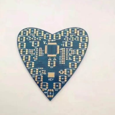


PCB boards mainly divided into single-layer PCB boards and double-layer PCB boards, as well as multi-layer PCB boards. The most commonly used are single-layer PCB and double-layer PCB boards, and those with more than three layers are called multilayer PCB boards. For applications in different industries, there are different requirements for its shape, size, color, model, number of layers, etc. Now let’s introduce the difference between single layer, double layer and multi layer PCB boards in detail.
- The difference in the number of layers:
To be simple, the main difference is single-sided wiring, double-sided wiring, and multilayer wiring.
1) single layer pcb:
one layer of medium, one side wiring;
2) double layer pcb:
one layer of medium, double-sided wiring;
3) multilayer PCB:
Usually at least 4 layers, multilayer medium, multilayer wiring.
- The difference in structure:The so-called single-sided PCB and double-sided PCB have different copper layers. A double-sided PCB has copper on both sides of the board, which can be connected through vias. However, a single-sided PCB has only one layer of copper, which can only be used for simple circuits, and the holes made can only be used for plug-ins and cannot be connected.
The single-sided printed circuit board is usually a single-sided copper clad laminate. The corroded circuit pattern is made on the copper surface by screen printing or photoimaging, and the excess copper foil is removed by chemical etching to form the conductor pattern. .
The double-sided printed circuit board has upper and lower conductor patterns, and the upper and lower layer are connected by holes. In the printed circuit board processing, the hole wall is plated with a copper layer to make the upper and lower layers conductive. The double-sided printed circuit board usually adopts double-sided copper clad laminates, using screen printing or photoimaging. A corrosion-resistant circuit pattern is made on the copper surface, and the excess copper foil is removed by chemical etching to form a conductor pattern.
The conductor pattern of the multilayer printed circuit board has three or more layers, and the conductor layer is divided into an inner layer and an outer layer. The inner layer is a conductor pattern completely sandwiched inside the multilayer board; the outer layer is a conductor pattern on the surface of the multilayer board. Generally, the inner conductor pattern is processed first during production, and the hole and the outer conductor pattern are processed after pressing, and the inner and outer layers are connected by metalized holes.
The production process of single-sided and double-sided circuit boards is basically similar, and the structure and production are relatively simple, while the multilayer circuit board is different. The requirements for structural design and process production of multilayer pcb are very high, the higher the number of layers, the difficulty is higher.